SPI NAND Protocolos compatibles
AlmacenamientoSPI NAND Flash
¿Qué es SPI NAND?
SPI NAND Flash combines NAND flash storage density with a simple SPI serial interface, providing a cost-effective storage solution for embedded systems that need more capacity than NOR flash but do not require a parallel NAND controller. SPI NAND devices use the same CLK, CS#, and IO0-3 signals as SPI NOR flash but implement the NAND command set with page-based read/program operations and block-based erase. The SPI interface operates at clock speeds up to 133 MHz in Quad I/O mode. Engineers debugging SPI NAND storage encounter challenges with page read sequences (command, address, dummy, data), ECC status interpretation, and bad block management that differ from the simpler NOR flash command model.
SPI NAND Referencia rápida
| type | Serial, synchronous |
| signals | CLK, CS, IO0-3 |
| max Speed | 133 MHz |
| voltage Range | 1.8V – 3.3V |
| features | SPI-interface NAND storage |
Instrumentos Acute compatibles con SPI NAND
Soluciones recomendadas
Recomendado para decodificación

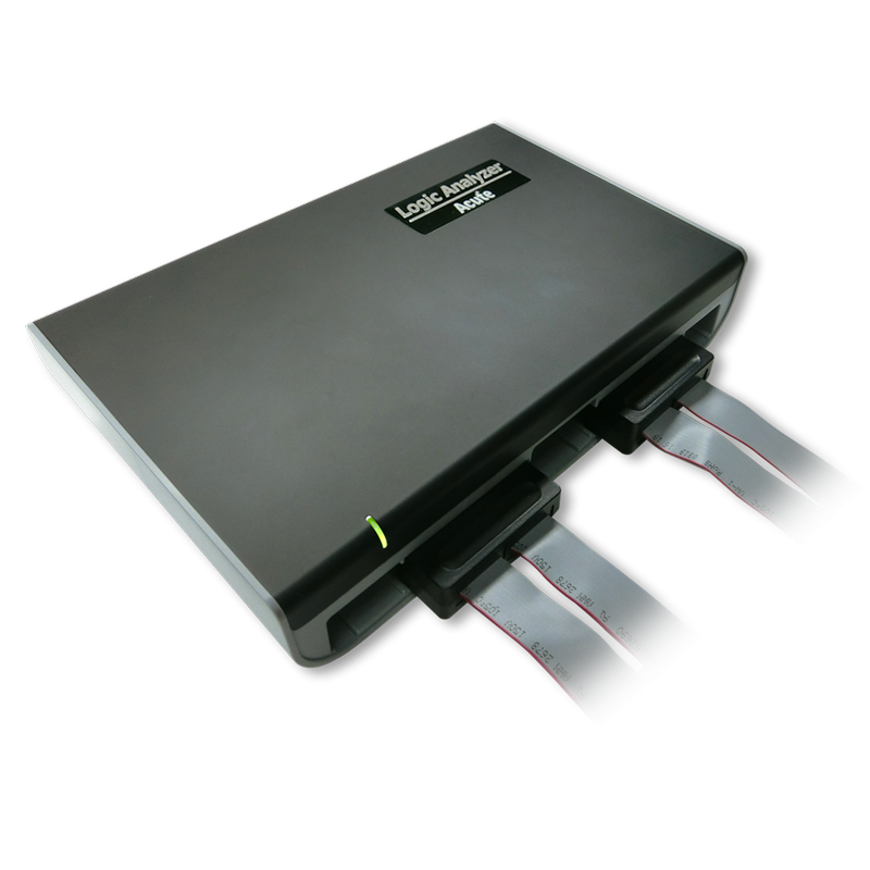
TL4234B
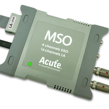
Todos los productos compatibles

¿Listo para analizar este protocolo?
Vea cómo los instrumentos Acute capturan y decodifican este protocolo en tiempo real. Solicite una demo o contacte a nuestro equipo.
¿Cómo analizar SPI NAND con instrumentos Acute
Conecte su analizador lógico Acute a las señales SPI NAND: CLK, CS#, IO0 (MOSI) y IO1 (MISO). Para modo Quad, conecte también IO2 e IO
Conecte un cable de tierra a la referencia de tierra de la placa objetivo.
En el software Acute, seleccione el SPI NAND protocol decoder y asigne cada señal al canal de entrada correspondiente.
Configure el decodificador para NAND device type and expected SPI mode (standard, Dual, or Quad).
Capture y visualice los SPI NAND commands showing page read, page program, block erase, and status register operations with address and data decoding.