SPI NAND Protocol Support
StorageSPI NAND Flash
What is SPI NAND?
SPI NAND Flash combines NAND flash storage density with a simple SPI serial interface, providing a cost-effective storage solution for embedded systems that need more capacity than NOR flash but do not require a parallel NAND controller. SPI NAND devices use the same CLK, CS#, and IO0-3 signals as SPI NOR flash but implement the NAND command set with page-based read/program operations and block-based erase. The SPI interface operates at clock speeds up to 133 MHz in Quad I/O mode. Engineers debugging SPI NAND storage encounter challenges with page read sequences (command, address, dummy, data), ECC status interpretation, and bad block management that differ from the simpler NOR flash command model.
SPI NAND Quick Reference
| type | Serial, synchronous |
| signals | CLK, CS, IO0-3 |
| max Speed | 133 MHz |
| voltage Range | 1.8V – 3.3V |
| features | SPI-interface NAND storage |
Acute Instruments Supporting SPI NAND
Recommended Solutions
Recommended for Decode

TL4234B
All Supporting Products

Ready to analyze this protocol?
See how Acute instruments capture and decode this protocol in real time. Request a demo or contact our team.
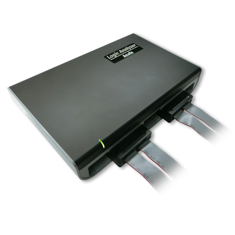
How to Analyze SPI NAND with Acute Instruments
Connect your Acute logic analyzer to the SPI NAND signals: CLK, CS#, IO0 (MOSI), and IO1 (MISO). For Quad mode, also connect IO2 and IO
Attach a ground lead to the target board's ground reference.
In the Acute software, select the SPI NAND protocol decoder and assign each signal to the correct input channel.
Configure the decoder for the NAND device type and expected SPI mode (standard, Dual, or Quad).
Capture and view decoded SPI NAND commands showing page read, page program, block erase, and status register operations with address and data decoding.