NAND Flash Protocol Support
StorageParallel NAND Flash Interface
What is NAND Flash?
Parallel NAND Flash is the raw interface used to communicate with NAND flash memory devices, providing direct access to the flash command set for read, program, erase, and status operations. The interface uses an 8-bit bidirectional data bus (IO[7:0]) along with control signals including CLE (Command Latch Enable), ALE (Address Latch Enable), WE# (Write Enable), RE# (Read Enable), and CE# (Chip Enable). Modern NAND flash devices conforming to ONFI 4.0 can operate at up to 200 MHz with DDR signaling. Engineers debugging embedded storage systems, SSD controllers, and NAND-based designs need parallel NAND analysis to verify command sequences, timing parameters, and data integrity at the flash interface level.
NAND Flash Quick Reference
| type | Parallel |
| signals | IO[7:0], CLE, ALE, WE, RE, CE |
| max Speed | 200 MHz (ONFI 4.0) |
| voltage Range | 1.8V / 3.3V |
| features | Raw NAND interface |


Ready to analyze this protocol?
See how Acute instruments capture and decode this protocol in real time. Request a demo or contact our team.
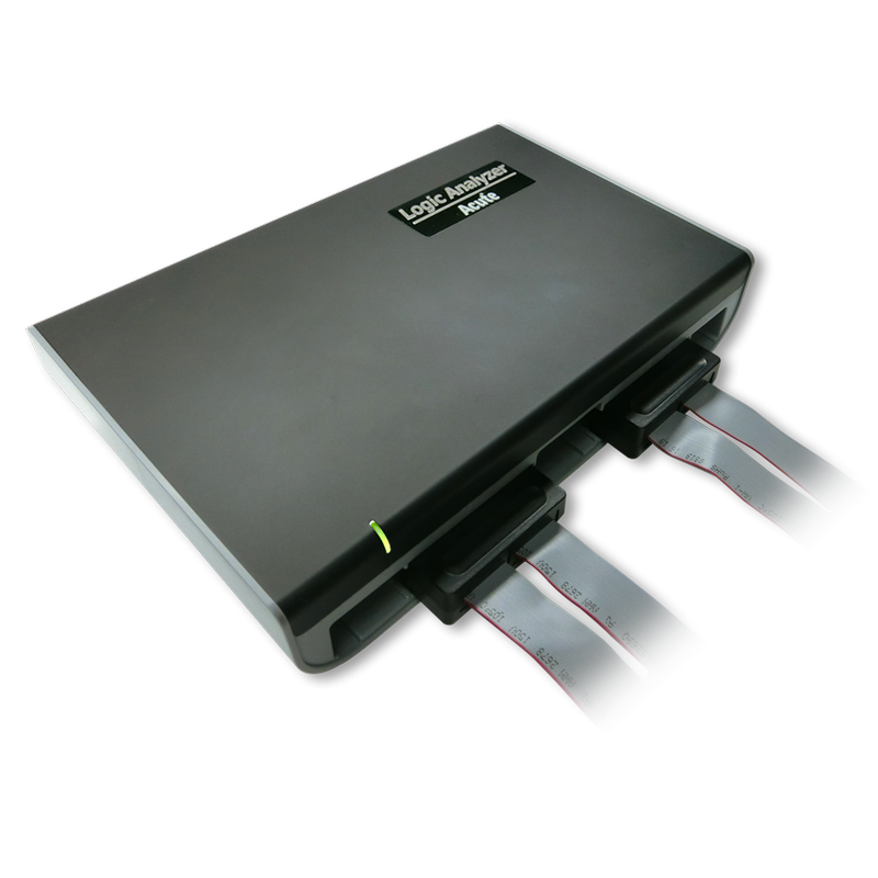
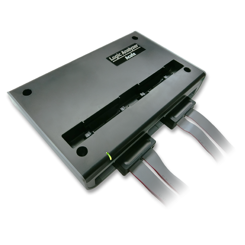
How to Analyze NAND Flash with Acute Instruments
Connect your Acute logic analyzer to the NAND flash signals: IO[7:0], CLE, ALE, WE#, RE#, CE#, and optionally R/B# (Ready/Busy).
Attach a ground lead to the target board's ground reference.
In the Acute software, select the NAND Flash protocol decoder and assign each signal to the correct input channel.
Configure the decoder for the NAND device type, addressing mode, and interface speed.
Capture and view decoded NAND commands, addresses, and data showing read, program, erase operations, and status responses.