NAND Flash Protocolos compatibles
AlmacenamientoParallel NAND Flash Interface
¿Qué es NAND Flash?
Parallel NAND Flash is the raw interface used to communicate with NAND flash memory devices, providing direct access to the flash command set for read, program, erase, and status operations. The interface uses an 8-bit bidirectional data bus (IO[7:0]) along with control signals including CLE (Command Latch Enable), ALE (Address Latch Enable), WE# (Write Enable), RE# (Read Enable), and CE# (Chip Enable). Modern NAND flash devices conforming to ONFI 4.0 can operate at up to 200 MHz with DDR signaling. Engineers debugging embedded storage systems, SSD controllers, and NAND-based designs need parallel NAND analysis to verify command sequences, timing parameters, and data integrity at the flash interface level.
NAND Flash Referencia rápida
| type | Parallel |
| signals | IO[7:0], CLE, ALE, WE, RE, CE |
| max Speed | 200 MHz (ONFI 4.0) |
| voltage Range | 1.8V / 3.3V |
| features | Raw NAND interface |
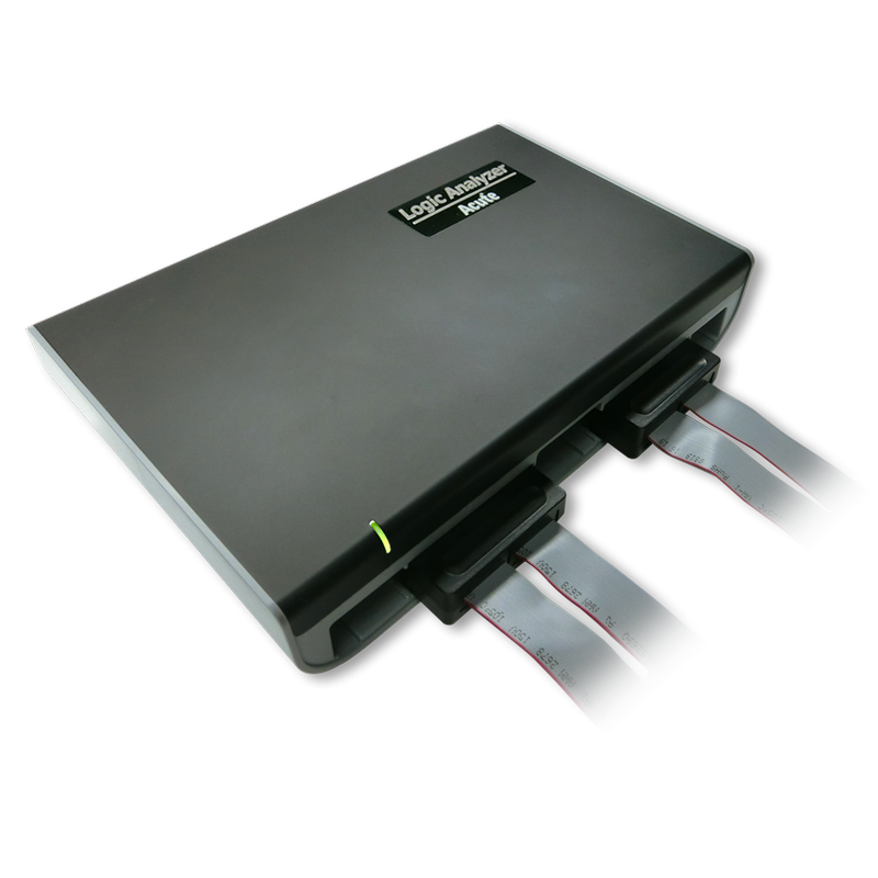
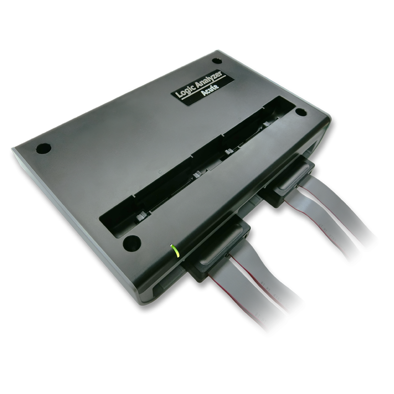
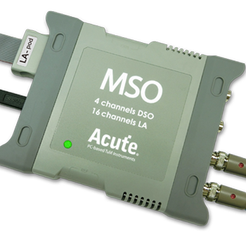
Instrumentos Acute compatibles con NAND Flash
Soluciones recomendadas

Todos los productos compatibles

¿Listo para analizar este protocolo?
Vea cómo los instrumentos Acute capturan y decodifican este protocolo en tiempo real. Solicite una demo o contacte a nuestro equipo.
¿Cómo analizar NAND Flash con instrumentos Acute
Conecte su analizador lógico Acute a las señales NAND flash: IO[7:0], CLE, ALE, WE#, RE#, CE# y opcionalmente R/B# (Ready/Busy).
Conecte un cable de tierra a la referencia de tierra de la placa objetivo.
En el software Acute, seleccione el NAND Flash protocol decoder y asigne cada señal al canal de entrada correspondiente.
Configure el decodificador para NAND device type, addressing mode, and interface speed.
Capture y visualice los NAND commands, addresses, and data showing read, program, erase operations, and status responses.