QSPI Protocol Support
StorageQuad SPI
What is QSPI?
QSPI (Quad SPI) is an enhanced version of the SPI protocol that uses four data lines instead of one, quadrupling the data throughput while maintaining the same clock frequency. QSPI is the predominant interface for NOR flash memory devices used to store firmware, boot code, configuration data, and application code in embedded systems, networking equipment, automotive ECUs, and consumer electronics. In QSPI mode, the traditional MOSI and MISO lines are repurposed as IO0 and IO1, with two additional lines IO2 and IO3 added for four-bit parallel data transfer. The protocol supports multiple operating modes — standard SPI (single I/O), Dual SPI (two I/O lines), and Quad SPI (four I/O lines) — and devices typically use single-I/O for command and address phases before switching to quad mode for the data phase. QSPI flash devices support clock rates up to 166 MHz in SDR mode and 100 MHz in DDR mode, achieving throughputs exceeding 400 Mb/s. Common QSPI operations include Read, Page Program, Sector Erase, Read Status Register, and various command sequences with configurable dummy cycles. Protocol analysis for QSPI is essential because flash memory failures during boot or runtime are difficult to debug without seeing the actual command sequences, address ranges being accessed, and data being transferred. Engineers need to verify correct command opcodes, address modes (3-byte vs 4-byte), dummy cycle counts, and XIP (Execute-In-Place) configuration.
QSPI Quick Reference
| type | Serial, synchronous |
| signals | CLK, CS, IO0-3 |
| max Speed | Up to 133 MHz |
| voltage Range | 1.8V – 3.3V |
| features | Quad I/O |
Acute Instruments Supporting QSPI
Recommended Solutions
With Analog Channels
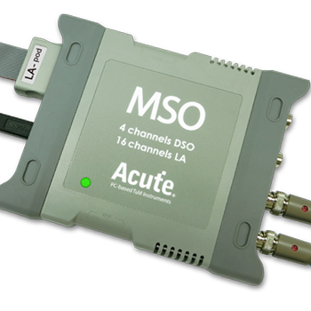
MSO2116E
only decode
All Supporting Products

Ready to analyze this protocol?
See how Acute instruments capture and decode this protocol in real time. Request a demo or contact our team.
How to Analyze QSPI with Acute Instruments
Connect your Acute logic analyzer to the QSPI signals: CLK, CS#, IO0, IO1, IO2, and IO
Attach a ground lead to the target board's ground reference.
In the Acute software, select the QSPI protocol decoder and assign each signal to the corresponding channel.
Configure the decoder for the flash device type or manually set the address width (3 or 4 bytes), data mode (single, dual, or quad), and DDR/SDR mode.
Capture and view decoded QSPI transactions showing command opcodes (Read, Program, Erase), addresses, dummy cycles, and data payloads for each chip-select-framed transaction.