JTAG Protocol Support
Embedded SystemsJoint Test Action Group (IEEE 1149.1)
What is JTAG?
JTAG (Joint Test Action Group) is a debug and test interface standardized as IEEE 1149.1, originally designed for boundary scan testing of circuit boards but now widely used for IC programming, debugging, and real-time trace in embedded systems. The JTAG interface uses a TAP (Test Access Port) with four required signals: TCK (Test Clock), TMS (Test Mode Select), TDI (Test Data In), and TDO (Test Data Out), plus an optional TRST (Test Reset). The TAP controller is a 16-state finite state machine driven by TCK and TMS, through which instructions and data are shifted in and out via TDI and TDO. JTAG supports shifting data through instruction registers (IR) to select operations, and through data registers (DR) to transfer data such as boundary scan patterns, device IDs, debug memory access, and breakpoint configurations. The protocol allows multiple devices to be daisy-chained on a single JTAG scan chain with TDO of one device connected to TDI of the next. JTAG is found in virtually every FPGA, ASIC, microprocessor, microcontroller, and complex SoC, making it one of the most important debug interfaces in electronics. Protocol analysis for JTAG is valuable for verifying scan chain integrity, debugging boundary scan test failures, analyzing debug port communication, and reverse-engineering device configurations. Engineers need to decode TAP state transitions, instruction register contents, and data register values to understand and troubleshoot JTAG communication.
JTAG Quick Reference
| type | Serial, synchronous |
| signals | TDI, TDO, TMS, TCK, TRST |
| max Speed | 10 – 100 MHz typical |
| voltage Range | 1.8V – 3.3V |
| features | Boundary scan |
Acute Instruments Supporting JTAG
Recommended Solutions
Recommended for Decode
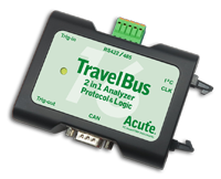
TB3016F
only decode
With Analog Channels
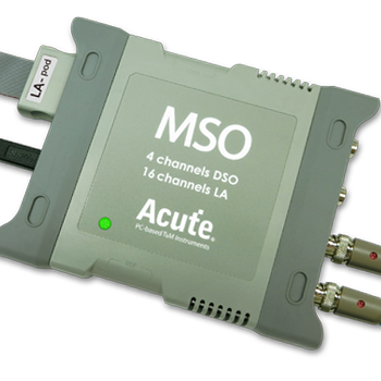
MSO2116E
only decode
All Supporting Products
Ready to analyze this protocol?
See how Acute instruments capture and decode this protocol in real time. Request a demo or contact our team.
How to Analyze JTAG with Acute Instruments
Connect your Acute logic analyzer to the JTAG signals: TCK, TMS, TDI, and TDO. Optionally connect TRST if present.
Attach a ground lead to the target board's ground, ideally at the JTAG header.
In the Acute software, select the JTAG protocol decoder and assign each signal to the corresponding channel.
Configure the decoder with the instruction register length (IR length) for each device in the scan chain.
Capture and view decoded JTAG activity showing TAP state transitions, instruction register values (BYPASS, IDCODE, EXTEST, etc.), data register shifts, and scan chain data for each device.